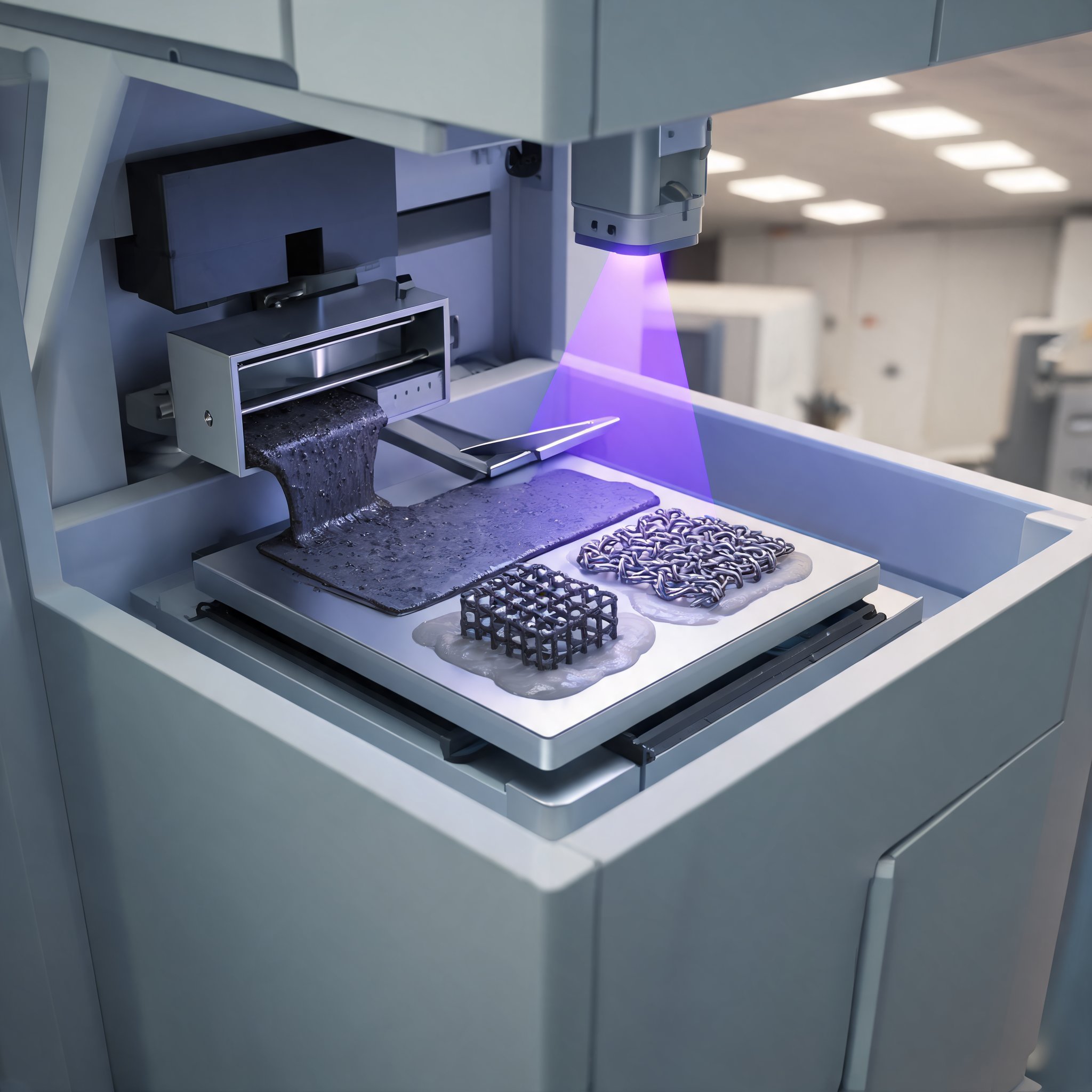
Researchers at Northwestern University have developed a hybrid 3D printing method called direct ink additive lithography, or DIAL, that aims to print thick, particle-filled inks with speed and planar resolution associated with light-based processes. The work, led by Pranav Kaarthik, was published in Science Advances.
The method addresses a trade-off between two established approaches. Digital light processing requires low-viscosity resins that scatter light only weakly, while direct ink writing can handle functional yield-stress inks but is constrained by filament deposition and nozzle diameter. DIAL combines extrusion with projection to work around those limits.
How the layer process works
For each layer, a slot die extrudes ink onto a substrate, and a doctor blade spreads it into a sheet as thin as 25 microns. A 405-nanometer projector then moves over the sheet and crosslinks selected regions. Ink that is not cured remains in place and acts as support. Because the light passes only through a thin sheet, opaque inks with heavy filler loading remain printable. The projector's 50-micron pixel pitch defines planar resolution.
Ryan Truby, the June and Donald Brewer Junior Professor of Materials Science and Engineering at Northwestern, said manufacturers have had to choose between the materials they need and the speed, resolution and scale they want. He described DIAL as a foundation for removing that compromise.
Printed demonstrations
Using a model ink made from a polyurethane-based resin thickened with fumed silica, the team printed a 60 mm by 40 mm log-pile structure in 30 minutes, compared with 124 minutes for direct ink writing. The process also produced fins about 150 microns thick. By rastering projection over overlaid ink sheets, the researchers made a multimaterial lattice covering four times the projector's illumination area.
Other demonstrations included interlocking chain mail with struts about 250 microns thick, 15 gyroid structural electrolyte lattices printed from an ionogel ink in one 15-minute run, and hydrogel cell culture inserts containing inverted pyramids 0.5 mm deep.
The authors described their reported print times as conservative because tool changes had not been optimized for speed. They also noted that the process does not involve the suction and peel forces found in vat-based printing, which they said should make it easier to expand build area and volume.
Path to manufacturing
Truby linked the work to broader manufacturing needs, saying that rebuilding American manufacturing will depend on new ways to make advanced materials. According to Truby, DIAL's ability to print many complex functional parts at once offers a route from laboratory demonstrations toward larger-volume production of architected materials for robotics, aerospace, healthcare and other applications.
Kaarthik and Truby are listed as coinventors on a U.S. provisional patent application. The work received funding from the National Science Foundation, the Air Force Office of Scientific Research and Northwestern's McCormick School of Engineering.